Pcb Designing (With 3D Model) In Orcad [2022]
Last updated 9/2022
MP4 | Video: h264, 1280x720 | Audio: AAC, 44.1 KHz
Language: English | Size: 10.83 GB | Duration: 12h 31m
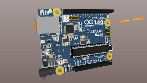
Schematic in OrCAD Capture CIS, Printed Circuit Board, BOM,Footprints, 3D Model,Routing and Gerber files for Arduino UNO
What you'll learn
Students can draw their own schematics and Design their own custom Printed Circuit Boards.
Students will learn basic terminologies related to PCB's that are used widely in books and industries
In Addition students will learn widely used electronics concepts
Requirements
Basic Concepts Of Electronics
Windows 10 (also works with Windows 7 & Windows 8) or Mac OS
I recommend to use a mouse if you are using Laptop
You will need a OrCAD & Cadence Allegro Software. If you are College/University student, you can ask for a student license (I recommend you use ORCAD free 30 Days trial)
In addition to educational packages for colleges and universities, OrCAD supports the student community by providing a Lite / student version of OrCAD (Student Version: The OrCAD Lite / Student product versions are not licensed, but instead are limited in terms of design size and complexity)
Description
Get Detailed introduction to Orcad Capture CIS, Pad-stack Editor and PCB Editor with Project-1 Project 1: Learn How to design basic Circuit based on real life projects[For beginners]Level Up your Skills with Project-2Project 2: Learn to design Schematic & PCB for Arduino UNO (includes multiple schematic pages, Off page connectors, search parts from Digi-Key, Professional Bill of material, Smart PDF for Schematic, How to download скачать custom footprints , How to create 3D Model etc )This course is complete & detailed walk through of industry leading PCB Design software. This course will help to develop a fundamentals in OrCAD, leading to better PCB design practices and skills. After completion of this course you will have skill and useful resources to design your own custom PCB's.This course is complete & detailed walk through of industry leading PCB Design software. This course will help to develop a fundamentals in OrCAD, leading to better PCB design practices and skills. After completion of this course you will have skill and useful resources to design your own custom PCB's.This course is complete & detailed walk through of industry leading PCB Design software. This course will help to develop a fundamentals in OrCAD, leading to better PCB design practices and skills. After completion of this course you will have skill and useful resources to design your own custom PCB's..
Overview
Section 1: Introduction & Installation
Lecture 1 Course Curriculum
Lecture 2 How to Install OrCAD Professional (2019)
Section 2:[For beginners] OrCad Capture CIS (2019)
Lecture 3 How to setup Project in OrCAD Capture
Lecture 4 Placing Parts, Wiring,Libraries,Symbols in OrCAD Capture Environment
Lecture 5 How to create custom Schematic symbols
Lecture 6 How to search symbols from Libraries
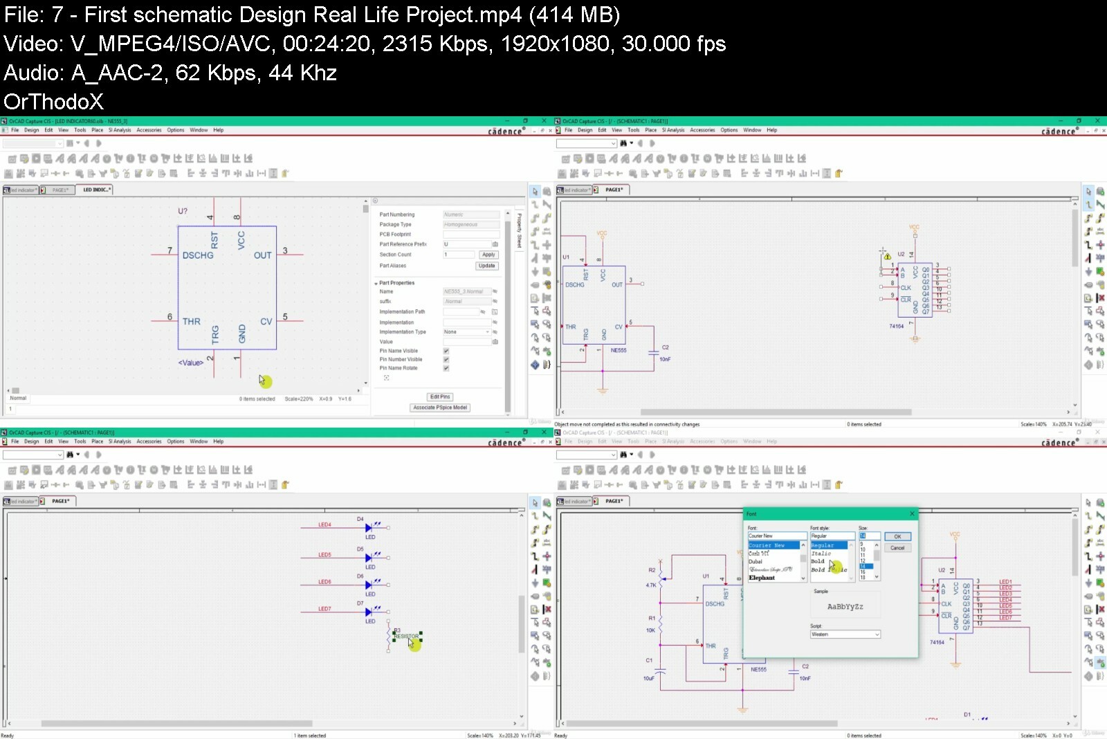
Lecture 7 First schematic Design (Real Life Project)
Lecture 8 How to assign footprints to schematic symbols
Lecture 9 Annotation, DRC, Netlist & Board File
Section 3:[For beginners] PCB Terminologies
Lecture 10 What is PCB
Lecture 11 What are Pads
Lecture 12 VIA (Vertical Interconnect Access)
Lecture 13 Plated vs Non Plated Holes
Lecture 14 What is Silkscreen
Lecture 15 What is SolderMask
Section 4:[For beginners] PCB Editor (2019)
Lecture 16 Introduction & Setup For PCB Editor
Lecture 17 How to setup Physical Rules (Constraint Manager)
Lecture 18 Requested Lecture (Physical Rules)
Lecture 19 PCB Layers (Cross_Section)
Lecture 20 How to place Components on PCB
Lecture 21 PCB Editor Custom Preferences
Lecture 22 How to Modify Footprints
Lecture 23 Board Outline & Mechanical symbols
Lecture 24 How To Update & Modify Board File
Lecture 25 PCB Routing Guidelines
Lecture 26 PCB Routing
Lecture 27 How to Setup Silkscreen
Lecture 28 Custom Text, Dimensions, NC Drill Legend....
Lecture 29 Gerber Files & NC Drill File
Lecture 30 Gerber Viewer
Section 5:[For beginners] Pad Stack Editor (2019) & Footprints
Lecture 31 Overview & Introduction of Padstack Editor
Lecture 32 How to Create Pads for Through Hole Resistor
Lecture 33 How to Create Footprint for Through Hole resistor
Lecture 34 How to Create Footprint for SMD Resistor
Lecture 35 Create Footprint for 555 Timer (DIP-8)[Through Hole]
Lecture 36 Footprint Layers (Important)
Lecture 37 Create Footprint for 555 Timer (DIP-8)[SMD]
Section 6:[Advanced] Arduino UNO Schematic in OrCAD Capture CIS (2019)
Lecture 38 download скачать Schematic & Project Setup in Capture CIS
Lecture 39 Schematic Symbols for ATMega328U & ATMega16UR
Lecture 40 Draw Schematic for AtMega328U & Wiring
Lecture 41 Reset Circuit & Decoupling Capacitor Schematic
Lecture 42 USB Bridge Schematic
Lecture 43 USB Circuit Schematic
Lecture 44 Net Naming (Alias) for AtMega328PU
Lecture 45 Net Naming (Alias) for USB Bridge Circuit
Lecture 46 Power Connector & voltage Regulator Circuit
Lecture 47 Power Selector Circuit
Lecture 48 Finishing our Arduino UNO Schematic
Section 7:[Advanced] Arduino UNO Components, Footprints & 3D Models from Digi-Key
Lecture 49 Component Properties Panel
Lecture 50 ATMega328PU Footprint & 3D Model
Lecture 51 ATMega16U2 Footprint & 3D Model
Lecture 52 Ceramic Capacitors Footprint(0805) & 3D Model (Part-1)
Lecture 53 Ceramic Capacitors Footprint(0805) & 3D Model (Part-2)
Lecture 54 Electrolytic Capacitors Footprint & 3D Model
Lecture 55 Diode Footprint & 3D Model
Lecture 56 LED Footprint(0805) & 3D Model
Lecture 57 Resistor Footprint(0805) & 3D Model
Lecture 58 Push Button Footprint & 3D Model
Lecture 59 Varistor Footprint & 3D Model
Lecture 60 5V Voltage Regulator Footprint (SOT223) & 3D Model
Lecture 61 3.3V (LDO) Voltage Regulator Footprint (SOT23) & 3D Model
Lecture 62 LM321 Footprint (SOT23) & 3D Model
Lecture 63 16MHz Crystal Footprint & 3D Model
Lecture 64 Ferrite Bead & Inductor Footprint & 3D Model
Lecture 65 N Channel Mosfet Footprint (SOT23) & 3D Model
Lecture 66 Female Headers Footprint & 3D Model
Lecture 67 USB Type B Connector Footprint & 3D Model
Lecture 68 12V DC Jack Connector Footprint & 3D Model
Lecture 69 ICSP Header Footprint & 3D Model
Section 8:[Advanced] PCB Editor (2019) Classes/Sub-classes
Lecture 70 Understanding Classes/sub-classes
Section 9:[Advanced] Fiducials & Mechanical symbols
Lecture 71 Create Schematic symbol for Fiducials and Mounting Holes
Lecture 72 Create Footprint for Fiducials and Mounting Holes
Section 10:[Advanced] Arduino UNO BOM, Smart PDF, Netlist and Board File
Lecture 73 Annotation, DRC, NetList and Board File
Lecture 74 Bill Of Material (BOM)
Lecture 75 Smart PDF of Schematic
Section 11:[Advanced ] Arduino UNO Component Placement
Lecture 76 PCB Editor Setup & Design Parameters
Lecture 77 Mounting Holes Placement
Lecture 78 Headers Placement
Lecture 79 ATMega328PU & Related Components Placement
Lecture 80 ATMega16U2 & Related Components Placement
Lecture 81 Rearrangement of Components
Lecture 82 Power Components Placement
Section 12:[Advanced] Arduino UNO Routing
Lecture 83 Physical Rules For Routing (Constraints)
Lecture 84 Routing Long Digital Connections (Part 1)
Lecture 85 Routing Long Digital Connections (Part 2)
Lecture 86 Route/ Track Glossing
Lecture 87 Routing Small Digital Connections
Lecture 88 Polygons/Shapes For Power Routing (Part 1)
Lecture 89 Polygons/Shapes For Power Routing (Part 2)
Lecture 90 Polygons/Shapes For Power Routing (Part 3)
Lecture 91 Polygons/Shapes For Power Routing (Part 4)
Lecture 92 Ground Plane Across The Board (Top Side)
Lecture 93 Ground Plane for Main Micro-controller (ATMega328)
Lecture 94 Ground Plane Across The Board (Bottom Side)
Lecture 95 Ground Plane for USB Bridge Micro-controller (ATMega16U2)
Lecture 96 Merge Shapes For Power Routing
Section 13: Lets Create 3D Model (Arduino UNO)
Lecture 97 Introduction to 3D View
Lecture 98 Mapping of 3D Models to Design Footprints (Part-1)
Lecture 99 Mapping of 3D Models to Design Footprints (Part-2)
Lecture 100 Lets do 3D Modeling
This course is very useful for students related to Electrical, Electronics and Computer Engineering . Also, this tool is worth to learn if you already have a knowledge about Altium Designer, Pads, Eagle or KiCAD,Engineering professionals who needs to learn and design their own printed circuit boards,Hobbyist, Entrepreneur and tech savvy people those are curious about PCB's
https://anonymz.com/?https://www.udemy.com/course/orcad2019/
https://rapidgator.net/file/bba47fa3a00a604c42d7e8cae7e7ffaa/PCB_Designing_with_3D_Model_in_Orcad_2022.part1.rar
https://rapidgator.net/file/90657719fe37303cb0db315636408f62/PCB_Designing_with_3D_Model_in_Orcad_2022.part2.rar
https://rapidgator.net/file/fecb7c62c7f8a2eb1822a7510a6058d8/PCB_Designing_with_3D_Model_in_Orcad_2022.part3.rar
https://nitroflare.com/view/46F49FBE956EB72/PCB_Designing_with_3D_Model_in_Orcad_2022.part1.rar
https://nitroflare.com/view/4E3A096D6ACD264/PCB_Designing_with_3D_Model_in_Orcad_2022.part2.rar
https://nitroflare.com/view/2EDDC7295A8A180/PCB_Designing_with_3D_Model_in_Orcad_2022.part3.rar